X
myLot
lameran
•
@lameran
(1147)
• Indonesia
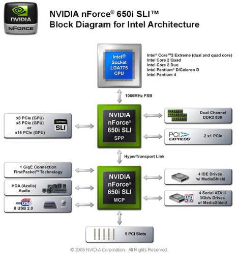
NVIDIA 650i block diagram for intel architecture. - NVIDIA has designed the 650i SLI as their true mainstream performance chipset, given the 680i is targeted to the upper end performance segment. The major highlights are the 650i only supports dual x8 SLI operation, single Gigabit Ethernet, four SATA 3Gb/s ports, and eight USB 2.0 ports instead of the dual x16 SLI, physics card slot, dual Gigabit Ethernet with teaming, six SATA 3Gb/s ports, and ten USB 2.0 ports on the 680i.